

Your CPU’s clock speed often 4–5 GHz in modern desktop processors¹ means it can execute billions of cycles per second. Yet main memory (RAM) can’t supply data at that furious pace. If the CPU had to wait for RAM on every instruction, it would spend most of its time idle, a bottleneck first described by John von Neumann. To bridge this gap, computer architects use a memory hierarchy of registers, cache, and RAM, each optimized for a different trade-off between speed, capacity, and cost.
Understanding the difference between these three layers is essential for anyone studying computer architecture or building high-performance systems.
What is the difference between RAM, cache, and registers?
The main differences are speed, size, and location:
- Registers are the fastest and smallest, built directly into the CPU core, and hold the data currently being processed.
- Cache is a small amount of high‑speed SRAM on the CPU die that stores frequently used data to reduce RAM access delays.
- RAM is larger, slower DRAM located on the motherboard, holding the entire working set of active programs.
In short, registers are the CPU’s workbench, cache is the nearby shelf, and RAM is the warehouse across the room.
Read our complete guide on computer hardware.
RAM, Cache, and Registers Compared
| Feature | Registers | Cache Memory (L1/L2/L3) | RAM (Main Memory) |
|---|---|---|---|
| Technology | Flip‑Flops (Logic Gates) | SRAM (Static RAM) | DRAM (Dynamic RAM) |
| Location | Inside CPU Core (ALU) | On CPU Die | Motherboard DIMM Slots |
| Latency | ~0‑1 Clock Cycle | ~3 – 50 Clock Cycles | ~200+ Clock Cycles |
| Size/Capacity | Bits to Bytes (e.g., 64‑bit) | Megabytes (e.g., 32MB) | Gigabytes (e.g., 32GB) |
| Data Stored | Active operands and instructions currently being processed by the ALU | Copies of recently used data and instructions from RAM | Full working set of operating system and running applications |
| Managed By | Compiler / Hardware | Hardware (Cache Controller) | Operating System / MMU |
| Speed | Fastest | Very Fast | Slow (Relative to CPU) |
| Cost per GB | Extremely High | High | Low |
The 5 Most Important Differences
- Speed: Registers (0‑1 cycle) > Cache (3‑50 cycles) > RAM (200+ cycles)
- Location: Registers inside CPU core → Cache on CPU die → RAM on motherboard
- Technology: Registers use flip‑flops, Cache uses SRAM, RAM uses DRAM
- Control: Registers (compiler), Cache (hardware), RAM (OS)
- Capacity: Registers (bytes) → Cache (MB) → RAM (GB)
Registers, cache, and RAM are three distinct layers of memory that a CPU uses to access data at different speeds and scales.
Registers sit inside the CPU core and hold the data being actively processed they operate in under one clock cycle. Cache sits between the CPU and RAM, storing recently or predictably needed data to reduce wait times; access takes 3 to 50 cycles depending on the cache level. RAM holds the full working set of running programs and is accessed in 200 or more clock cycles, making it the slowest of the three but by far the largest in capacity.
The hierarchy exists because no single memory technology can simultaneously be fast, large, and affordable. Each layer makes a different trade‑off.
Inside Registers, Cache, and RAM: How Each Memory Layer Works
Registers — The CPU’s Workbench
A register is a small, high‑speed storage location built directly into the CPU’s execution core. The Arithmetic Logic Unit (ALU) can only perform operations addition, comparison, logical shifts on data that is already in a register. Every calculation a CPU performs passes through registers. Typical registers include the Accumulator, Program Counter, Instruction Register, and Memory Address Register. A typical 64‑bit processor has between 16 and 32 general‑purpose registers, each 64 bits wide. Total register capacity is measured in bytes, not kilobytes.
Cache Memory — The Invisible Bridge
Cache is a pool of fast SRAM memory located on the CPU die, organized into levels (L1, L2, L3). Its job is to hold copies of data from RAM that the CPU is likely to need soon. Because cache operates orders of magnitude faster than RAM, a well‑populated cache can make a slow memory system feel nearly invisible to the processor. The CPU manages cache automatically; programmers and users have no direct control over what it stores.
RAM — The System Workspace
RAM is the primary workspace for the operating system and all running applications. It holds the full contents of open programs, active files, and OS data structures. Unlike registers and cache, RAM is measured in gigabytes and sits on physical modules (DIMMs) connected to the motherboard. It is significantly slower than cache but far cheaper per gigabyte, which is why it provides the bulk of a system’s working memory capacity.
All three memory types are volatile: they lose their contents the moment power is removed. For persistent storage, data must be written to an SSD or hard drive.
The Physical Difference: SRAM vs DRAM
The most common confusion regarding memory is why we don’t simply build a computer with 32GB of the fastest available memory (Registers) and ditch the slower RAM entirely.
The answer lies in the physics of how bits are stored.
Registers and Cache use SRAM (Static Random Access Memory).
SRAM stores data using flip‑flop circuits, typically requiring 6 transistors per bit. It is incredibly fast and stable it doesn’t need to be refreshed to keep its data. However, because it requires 6 transistors for a single bit, it takes up a massive amount of physical space on the silicon die.
RAM uses DRAM (Dynamic Random Access Memory).
DRAM stores data using capacitors. It is much simpler, requiring only 1 transistor and 1 capacitor per bit. This allows engineers to pack billions of bits into a small chip (high density). However, capacitors leak charge. They must be electronically “refreshed” thousands of times per second, which creates latency and overhead.
The Engineering Constraint:
If you tried to build 32GB of storage using the 6‑transistor SRAM found in registers, the chip would be the size of a pizza box, cost thousands of dollars, and generate enough heat to melt through your motherboard. We use DRAM for main memory not because we want to, but because it is the only way to get gigabytes of capacity at a viable size and price.
How Data Moves Between RAM, Cache, and Registers
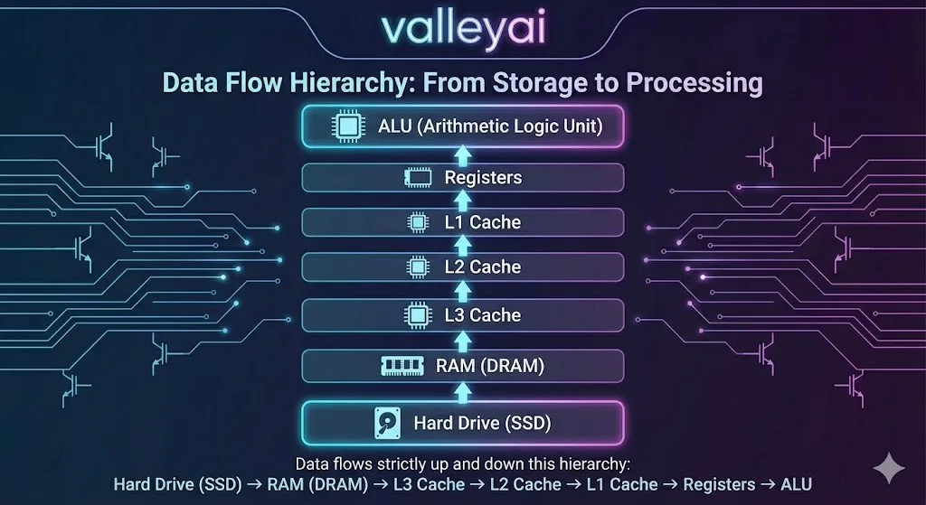
Here is the step‑by‑step path data takes from storage to the CPU’s execution units:
- SSD / Hard Drive (persistent storage, slowest)
- RAM (working memory, holds full program)
- L3 Cache (shared across cores, large but slower than L1/L2)
- L2 Cache (dedicated to a single core, faster than L3)
- L1 Cache (immediately adjacent to execution units, minimal latency)
- Registers (inside the ALU; the only memory the CPU operates on directly)
Data always moves up this chain before a CPU can use it. The hierarchy exists to mask the latency gap between the slow bottom and the fast top.
RAM (The Staging Area):
The Operating System loads the entire program and its data from the SSD into RAM. RAM is large enough to hold the full context of the application, but it is far away from the CPU core in terms of clock cycles. Fetching data from here takes roughly 100 nanoseconds. To a 4GHz CPU, that is an eternity.
Cache (The Prediction Layer):
The CPU’s hardware logic anticipates what data the processor will likely need next (based on locality algorithms) and pulls a copy of it from RAM into the Cache.
- L3 Cache: Shared by all cores. Large but slightly slower.
- L2 Cache: Dedicated to a specific core.
- L1 Cache: Extremely small, integrated directly next to the execution units. Accessing L1 cache takes only 1 to 3 clock cycles.
Registers (The Workbench):
This is the destination. Before the CPU can actually add those two numbers, the data must be moved from the Cache into the Registers. Registers are the only memory the Arithmetic Logic Unit (ALU) can work with directly. They hold the immediate operands (the actual numbers being added) and the result. Access is instantaneous (0‑1 clock cycle).
How Each Memory Type Operates: Control, Speed, and Capacity Trade‑offs
Let’s breakdown the difference between ram cache and registers.
Registers: The Architect’s Tools
Registers are the fastest, smallest, and most expensive memory in the system. They are located inside the CPU core itself.
- Capacity: Measured in bits. A 64‑bit processor has general‑purpose registers that are 64 bits wide. The total volume of register space is minuscule (often less than a few kilobytes).
- Control: Compiler‑Controlled. When code is compiled from C++ or Rust into Assembly, the compiler explicitly decides which variables go into which registers. The programmer (or their compiler) has direct control here.
- Role: They hold the active state of the CPU the instruction pointer, the stack pointer, and the variables currently being mathematically manipulated.
Cache: The Invisible Bridge
Cache is designed to hide the latency of RAM. It works automatically; you cannot write code that says “save this variable to L1 Cache.”
- Capacity: Measured in Kilobytes (L1/L2) to Megabytes (L3).
- Control: Hardware‑Controlled. The CPU has dedicated circuits that manage cache lines. If the CPU asks for data and it’s found in the cache, it’s a cache hit. If not, it’s a cache miss, and the system must stall while fetching from RAM.
- Role: It acts as a buffer. Because programs tend to access memory sequentially, the cache grabs blocks of data (cache lines) anticipating they will be used soon.
RAM: The System Workspace
RAM is the primary workspace for the operating system and all active programs.
- Capacity: Measured in Gigabytes (8GB, 16GB, 64GB).
- Control: OS‑Controlled. The operating system allocates memory addresses and manages which programs occupy which regions via the Memory Management Unit (MMU).
- Role: Holds the full working set of running applications, preventing the system from reading from the far slower SSD or hard drive.
Memory bandwidth: the rate at which data can be transferred between RAM and the CPU is a separate constraint from latency. Modern DDR5 RAM offers bandwidths exceeding 50GB/s², yet even that throughput becomes a bottleneck when multiple CPU cores simultaneously demand data. This is one reason why on‑chip cache, which can deliver hundreds of GB/s of effective bandwidth, remains so valuable even as RAM speeds improve.
Why Cache Works: Spatial and Temporal Locality Explained
The hierarchy relies on a principle called Locality of Reference. Without this, the cache would be useless.
Spatial Locality: If a program accesses memory address 100, it is highly likely to access address 101 next. (Think of reading an array or a list sequentially). The cache loads 100 through 128 automatically, so the next requests are instant.
Temporal Locality: If a program uses a variable x now, it will likely use x again very soon (think of a loop counter). The cache keeps recently used data ready for reuse.
Because code is generally predictable, a small amount of Cache (e.g., 32MB) can successfully serve the CPU’s needs 95% of the time, making the slow RAM feel much faster than it actually is.
Volatility: Why RAM, Cache, and Registers Lose Data When Power Is Off
Registers, cache, and RAM are all volatile memory meaning their contents are erased the moment power is cut. This distinguishes them from SSDs and hard drives, which retain data without power. When a computer crashes or shuts down unexpectedly, any data that had not yet been written from RAM to persistent storage is lost. This is why applications save working files to disk rather than relying on RAM alone.
How Modern Architectures Are Changing the Memory Hierarchy
The rigid distinction between these layers is beginning to evolve. AMD’s 3D V‑Cache technology stacks additional SRAM vertically on top of the processor die, creating L3 caches of up to 192MB on consumer CPUs³. This dramatically reduces how often the CPU must reach out to slower RAM a meaningful advantage in gaming workloads where game physics and geometry data fits within the expanded cache.
Apple’s Unified Memory Architecture takes a different approach: rather than separating CPU and RAM onto different physical packages, it places DRAM on the same silicon package as the CPU and GPU. This reduces the physical distance data must travel and narrows the latency gap between cache and main memory, though the fundamental hierarchy (registers → cache → RAM) still exists within the architecture.
A third emerging development is Processing‑in‑Memory (PIM), where computational logic is embedded directly inside DRAM chips, reducing the need to move data to the CPU at all. Samsung and SK Hynix have both demonstrated PIM prototypes⁴. Whether this approach becomes mainstream remains to be seen, but it signals that the classical memory hierarchy is under active re‑examination.
The core constraint a small amount of ultra‑fast storage for immediate work, a large amount of slower storage for capacity will persist. What changes is how aggressively engineers compress the distance between those extremes.
Final Thoughts: The Unavoidable Trade‑Off
The memory hierarchy is a compromise between speed, cost, and capacity. No single technology can replace all three. Registers give the CPU instant access to a handful of values, cache hides the gap to RAM, and RAM provides the gigabytes of space modern software demands. Grasping these differences is the first step toward understanding how computers execute billions of operations without stalling.
FAQs:
What is the physical location of registers and cache?
Registers are physically embedded inside the CPU execution cores (often next to the ALU). L1 and L2 Cache are also inside the core. L3 Cache is usually shared between cores on the CPU die. RAM is located on separate modules (sticks) plugged into the motherboard, communicating via the Memory Controller Hub.
Is register faster than cache memory?
Yes. Registers are faster than cache memory. A register access completes in less than one CPU clock cycle. L1 cache the fastest cache level requires 3 to 5 cycles. L2 cache takes roughly 10 to 15 cycles, and L3 cache can take 30 to 50 cycles depending on the processor architecture. Registers operate at the full internal frequency of the CPU with no intermediary step.
Why do we need cache if we have registers?
Density and Cost. Registers are built using Flip‑Flops, which are physically large and power‑hungry. If we tried to build 32GB of memory using Flip‑Flops (Registers), the CPU would be the size of a dinner table and cost millions. We use Cache and RAM as a compromise between speed, size, and cost.
How does cache locality affect program speed?
Cache locality affects speed by maximizing Cache Hits and minimizing Cache Misses. When a program accesses memory sequentially (good spatial locality), the CPU finds the data in the L1/L2 cache rather than waiting hundreds of cycles to fetch it from RAM. Poor locality causes the CPU to stall (stop working) while waiting for data.
Is RAM more important than CPU cache for gaming?
For smoothness (1% low FPS), CPU Cache (specifically 3D V‑Cache or large L3) is often more important. Large L3 cache keeps complex game physics and geometry data close to the core, preventing stutter. However, you need enough RAM (capacity) to hold the game assets. If you run out of RAM, the system swaps to the SSD, which destroys performance.
High Cache: Higher max FPS, less stutter.
High RAM Capacity: Prevents crashes and massive lag spikes.
What is volatile memory?
Volatile memory is any memory that loses its stored data when power is removed. Registers, cache, and RAM are all volatile. This is why unsaved work disappears during a power outage the data existed in RAM but had not yet been written to an SSD or hard drive, which are non‑volatile. All three memory types discussed in this article are volatile by design.
Is RAM faster than cache?
No. RAM is significantly slower than any level of CPU cache. Cache uses SRAM, which does not require periodic refreshing and sits on the CPU die. RAM uses DRAM, which must be electrically refreshed thousands of times per second and communicates with the CPU across a physical bus on the motherboard. The result: even the slowest cache level (L3) is typically 4 to 10 times faster than RAM in terms of access latency.
What is the difference between CPU cache and RAM?
The main difference is volatility technology and proximity. Cache uses SRAM (fast, complex, on‑chip) to store frequently used data. RAM uses DRAM (slower, dense, off‑chip) to store the bulk of running program data.
Can I upgrade my CPU Cache?
No. L1, L2, and L3 cache are soldered directly onto the CPU die. To get more cache, you must buy a different CPU (e.g., upgrading to an AMD X3D model or an Intel Extreme edition).
Do registers store instructions or data?
Both. There are General Purpose Registers (GPR) for data (like integers) and Special Purpose Registers (like the Instruction Pointer or Program Counter) that track which line of code acts next.
What happens if Cache is full?
The Cache Controller uses an eviction policy, typically LRU (Least Recently Used). It looks at the data that hasn’t been touched in a while, writes it back to RAM (if modified), and deletes it from the Cache to make room for new data.
Further Reading
- Intel® 64 and IA‑32 Architectures Software Developer’s Manual
- AMD Official Technical Documentation
- JEDEC DDR5 SDRAM Standard
¹ Based on Intel® Core™ i9‑14900K specifications.
² JEDEC DDR5‑6400 standard bandwidth.
³ AMD 3D V‑Cache announcement, AMD.com.
⁴ Samsung PIM press release, Samsung Newsroom.
DDR generations in detail: what DDR stands for, what we know about DDR6, and what happens when your RAM is full.

Kaleem
My name is Kaleem and i am a computer science graduate with 5+ years of experience in Computer science, AI, tech, and web innovation. I founded ValleyAI.net to simplify AI, internet, and computer topics also focus on building useful utility tools. My clear, hands-on content is trusted by 5K+ monthly readers worldwide.