In the world of high-performance computing, raw clock speed is no longer the sole dictator of performance. The true bottleneck is often latency. While modern CPUs operate in the gigahertz range (billions of cycles per second), system RAM (DRAM) is comparatively sluggish.
If a CPU had to wait for system RAM for every single instruction, a 5.0 GHz processor would spend most of its life idling. This phenomenon is known as the Von Neumann Bottleneck.
CPU Cache is the hardware solution to this latency gap. It is a small, ultra-fast block of memory located directly on or near the processor die, utilizing SRAM (Static Random Access Memory). Unlike DRAM, which requires constant refreshing and uses capacitors, SRAM uses flip-flop circuits to hold data, making it significantly faster but more expensive and less dense.
The goal of the cache hierarchy is simple: Keep the execution units fed.
What Are CPU Cache Levels?
CPU cache levels are tiers of ultra-fast memory built directly into a processor, designed to reduce the time a CPU spends waiting for data. Each level L1, L2, and L3 sits closer to or farther from the execution core, trading speed for capacity. L1 is the smallest and fastest; L3 is the largest and slowest of the three. Together, they form a memory hierarchy that keeps the processor supplied with data without constantly accessing slower system RAM.
How Does the Memory Hierarchy Work in Plain Terms?
The Workshop Analogy:
Imagine a carpenter (the CPU Core) working in a workshop.
- L1 Cache: The toolbelt around their waist. Immediate access, but holds very little.
- L2 Cache: The tool chest on the workbench. Arms-reach access, holds more tools.
- L3 Cache: The supply closet in the hallway. Shared by all carpenters in the building, holds bulk materials.
- RAM: The warehouse across town. Getting anything from here stops work completely (high latency).
What is L1 Cache and Why is it the Fastest Memory?
The Hot Zone
The Level 1 (L1) Cache is the first line of defense against latency. It is physically embedded inside the CPU core, making it the fastest memory in the entire computer system.
How is L1 Cache Split into L1i and L1d?
In almost all modern architectures (including AMD Zen 5 and Intel Raptor Lake), the L1 cache is split:
- L1 Instruction Cache (L1i): Stores the actual opcodes (instructions) the CPU needs to execute next.
- L1 Data Cache (L1d): Stores the data those instructions will manipulate.
This split is critical for instruction pipelining, allowing the CPU to fetch instructions and data simultaneously (Harvard Architecture modification).
Key Characteristics (2024-2025 Standards):
- Size: Typically very small (32KB to 64KB per core). Increasing L1 size increases latency, so architects keep it tight.
- Latency: Instantaneous. Usually 3-4 clock cycles (approx. 0.7 – 0.9 nanoseconds on a 5GHz chip).
- Associativity: Highly associative (often 8-way or 12-way), meaning data can be stored in multiple valid locations to reduce conflict misses.
Hardware Prefetching: How the CPU Predicts What You’ll Need Next
Modern CPUs do not wait passively for cache misses. The hardware prefetcher monitors memory access patterns and speculatively loads data into cache before the core explicitly requests it. If code accesses array elements sequentially, the prefetcher detects the stride pattern and begins fetching ahead, often eliminating the miss penalty entirely.
Prefetching is most effective with predictable, linear access patterns one reason the cache-friendly code patterns in the developer section below matter so much in practice.
What is L2 Cache and How Does it Buffer Core Speed and System Limits?
The Bridge Between Core and System
The Level 2 (L2) Cache acts as the primary buffer for the L1. While early CPUs (like the Pentium II) had L2 on the motherboard or a separate daughter card, modern L2 is strictly on-die.
Why Has L2 Cache Capacity Expanded in Recent Generations?
In recent generations (Zen 5 and Raptor Lake), we have seen a massive ballooning of L2 sizes. Why? Because the penalty for missing the L2 and going to L3 (or RAM) has become too costly for modern, complex workloads like AI inference and high-refresh-rate gaming.
- Intel Raptor Lake: Moved to 2MB per core on Performance Cores.
- AMD Zen 5: Maintains 1MB per core, prioritizing lower latency over raw size, utilizing a different victim-cache topology.
Architecture Nuance:
The L2 is generally unified (storing both instructions and data) and is usually private to each core. However, Intel’s Efficient Cores (E-Cores) share clusters of L2 cache to save die space.
Write-Through vs Write-Back: How Cache Handles Data Updates
When a CPU modifies data, the cache must decide when to update the copy in the next memory tier. Two policies govern this:
Write-through sends the update immediately to the next cache level (or RAM). This keeps all tiers synchronized but generates more memory traffic.
Write-back marks the cache line as “dirty” and delays writing the update until that line is evicted. This reduces memory bus traffic significantly but requires the cache controller to track which lines have been modified.
Modern x86 architectures (AMD Zen and Intel Core) use write-back as the default policy for L1 and L2 caches because of its performance advantage. Write-through is more common in embedded systems where data consistency under power loss is a priority.
L3 Cache: The Shared Last Level Cache (And Why Size Matters)
The Shared Last Level Cache (LLC)
The Level 3 (L3) Cache, often called the Last Level Cache (LLC), is the final stop before the CPU must request data from system RAM. Unlike L1 and L2, the L3 is generally shared across all cores.
Interconnects and Coherence
Because L3 is shared, the CPU uses complex interconnects (like Intel’s Ring Bus or AMD Infinity Fabric) to manage data flow. This introduces the challenge of Cache Coherence ensuring that if Core 1 modifies data in the L3, Core 2 doesn’t read an outdated version. Protocols like MESI (Modified, Exclusive, Shared, Invalid) manage this.
What is the Innovation Behind AMD 3D V-Cache?
One of the most significant hardware shifts in the 2020s is vertical cache stacking. Standard L3 cache is laid out horizontally on the silicon (2D).
- The Technology: AMD 3D V-Cache uses TSMC’s hybrid bonding to stack an additional slice of SRAM directly on top of the existing L3 cache region.
- The Impact: This triples the L3 capacity (e.g., from 32MB to 96MB) without changing the motherboard footprint.
- Why it Matters: In gaming, main threads often wait for geometry or physics data. A massive L3 prevents the CPU from accessing slow RAM, resulting in significant improvements in 1% Low FPS and overall smoothness.
What are L4 Cache and eDRAM?
A small number of processor designs have included an L4 cache layer. Intel’s Broadwell-H and Skylake-H mobile processors used embedded DRAM (eDRAM) as a large, relatively fast L4 cache (up to 128MB) to reduce the power cost of accessing off-package RAM. This approach was discontinued as on-die L3 capacity grew and 3D V-Cache offered a more efficient stacking solution.
For desktop and server CPUs in 2024–2025, L3 remains the last on-die cache level in mainstream architectures. L4 is not a concept you need to account for in modern desktop CPU selection.
Comparative Data Table: Nanoseconds vs Cycles
The following table benchmarks typical latencies for current-generation architectures (Architecture Year 2024/2025).
| Hierarchy Level | Memory Type | Typical Size (Per Core/Shared) | Latency (Cycles) | Latency (Time @ 5GHz) | Primary Purpose |
|---|---|---|---|---|---|
| L1 Cache | SRAM (Split) | 32KB – 48KB (Private) | 3 – 5 cycles | 0.6 – 1.0 ns | Immediate execution instructions & hot data variables. |
| L2 Cache | SRAM (Unified) | 1MB – 2MB (Private) | 12 – 16 cycles | 2.4 – 3.2 ns | Buffering L1 evictions; preventing pipeline stalls. |
| L3 Cache | SRAM (Shared) | 32MB – 96MB+ (Shared) | 40 – 80 cycles | 10 – 16 ns | Data synchronization between cores; large dataset working sets. |
| System RAM | DDR5 DRAM | 16GB – 64GB (System) | 250 – 400+ cycles | 60 – 90 ns | Bulk storage of active applications and OS kernel. |
Which Cache Level Is Fastest?
L1 cache is always the fastest, typically delivering data in 3–5 clock cycles (under 1 nanosecond on a 5 GHz processor). L3 cache, by comparison, takes 40–80 cycles roughly 10–16 times slower. The tradeoff is capacity: L1 holds kilobytes per core, while L3 holds tens to hundreds of megabytes shared across all cores. Speed decreases and capacity increases at each level, which is why the hierarchy exists at all.
Engineers Note: Notice the jump from L3 to RAM. Going from 16ns to 80ns is a cache miss penalty that devastates performance. This is why 3D V-Cache is effective it keeps more data in the 16ns zone.
How Much CPU Cache Do You Actually Need?
Cache requirements vary significantly by workload. The table below summarizes practical guidance:
| Gaming | L3 (large working set, random access) | 32MB+ L3; 3D V-Cache beneficial above 96MB |
| Video editing / rendering | Less cache-dependent (streaming data) | Clock speed matters more |
| Database / server workloads | L3 (frequent random lookups) | As much as available |
| Software development / compilation | L2 + L3 | 1MB+ L2 per core; 16MB+ L3 |
| General productivity | L1 + L2 sufficient | Standard configurations adequate |
For gaming specifically, AMD’s 3D V-Cache chips (Ryzen 7 7800X3D, Ryzen 9 9950X3D) consistently outperform higher-clocked alternatives in titles that stress random memory access a direct result of L3 capacity advantages over raw frequency.
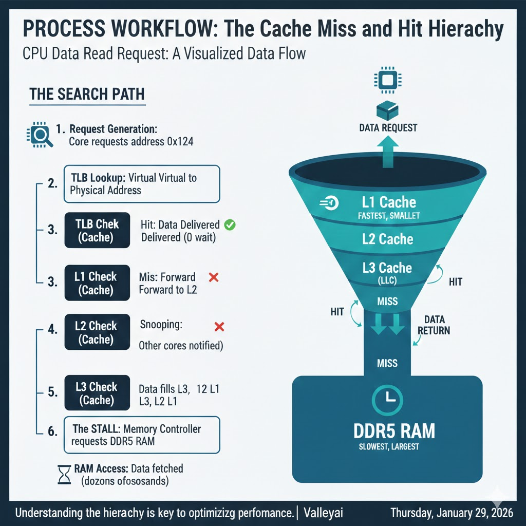
How a CPU Finds Data: Cache Hits, Misses, and the Memory Lookup Chain
When a CPU needs data, it searches each cache level in sequence L1 first, then L2, then L3 before falling back to system RAM. Finding data at any cache level is called a cache hit; failing to find it is a cache miss. Each miss escalates to the next, slower tier. Because L1 operates in under 1 nanosecond while RAM can take 80+ nanoseconds, the difference between a hit and a miss at the right level determines whether a workload runs smoothly or stalls.
What is the CPU’s Search Path for Data?
- Request Generation: The Core requests data address
0x1234. - TLB Lookup: The translation lookaside buffer converts the virtual address to a physical address.
- L1 Check:
- Hit: Data delivered immediately (0 wait).
- Miss: Request forwarded to L2.
- L2 Check:
- Hit: Line copied to L1, data delivered.
- Miss: Request forwarded to L3.
- L3 Check (LLC):
- Hit: Line copied to L2 and L1. Snooping ensures other cores know this data is being touched.
- Miss: The stall. The Memory Controller requests data from DDR5 RAM.
- RAM Access: The CPU waits dozens of nanoseconds. Data is fetched, filling L3, L2, and L1 lines on its way back to the core.
How Can We Visualize the Cache Hierarchy?
Imagine a funnel. The top (L1) is narrow but fast. The bottom (RAM) is wide but slow. Data must flow up the funnel to reach the CPU.
Writing Cache-Friendly Code: Spatial and Temporal Locality
For software developers, understanding cache is the difference between code that runs and code that flies. You cannot manually manage cache (the hardware handles that), but you can write cache-friendly code.
1. What is Spatial Locality (The Neighbor Rule)?
The CPU rarely fetches a single byte; it fetches a cache line (usually 64 bytes). If you request byte 0, the CPU fetches bytes 0-63.
- Optimization: Use contiguous memory arrays.
- Pattern: Structure of Arrays (SoA) often outperforms Array of Structures (AoS).
- Bad (AoS):
Array[1000] of {x, y, z, r, g, b, hp, name}. Looping through justxloads unnecessary data (hp,name) into the cache, wasting space. - Good (SoA):
Array_X[1000],Array_Y[1000]. Looping throughxfills the cache line only with relevantxvalues.
- Bad (AoS):
2. What is Temporal Locality (The Reuse Rule)?
If you use a variable, you are likely to use it again soon.
- Optimization: Complete all operations on a specific dataset block before moving to the next.
- Technique: Loop tiling (blocking). Instead of iterating over a massive matrix row by row (which evicts the start of the row from L1 before you return), break the matrix into small tiles that fit entirely inside L1 cache.
// Example: Cache Unfriendly (Row-major traversal vs Col-major storage)
for (int j = 0; j < N; j++) {
    for (int i = 0; i < N; i++) {
        data[i][j] = data[i][j] * 2; // Jumping memory locations causes L1 misses
    }
}

// Example: Cache Friendly (Linear access)
for (int i = 0; i < N; i++) {
    for (int j = 0; j < N; j++) {
        data[i][j] = data[i][j] * 2; // Sequential access maximizes Spatial Locality
    }
}
CPU Cache Levels: Key Takeaways
The three cache levels in a modern CPU serve a single purpose: keeping the processor supplied with data fast enough that execution units never sit idle.
- L1 is the fastest and smallest private to each core, measured in kilobytes, latency under 1 nanosecond.
- L2 acts as the buffer larger, slightly slower, still private in most designs, measured in megabytes.
- L3 is the shared pool the last line of defense before slow system RAM, measured in tens to hundreds of megabytes.
- Cache misses at any level are the primary cause of CPU stalls in real workloads.
- For developers, writing cache-friendly code (linear access, data structure layout) is one of the highest-leverage performance optimizations available without changing hardware.
- For buyers, L3 cache size matters most for gaming and latency-sensitive workloads; for rendering and encoding, clock speed and core count typically dominate.
FAQ: Common Questions on Cache Architecture
How does 3D V-Cache improve gaming performance?
AMD 3D V-Cache improves gaming performance by dramatically increasing L3 cache capacity (from ~32MB to 96MB+), keeping more game data on-die and reducing how often the CPU must wait for system RAM. Games with large, unpredictable data access patterns physics, AI, draw calls benefit most. The result is smoother frame times and higher 1% low FPS, particularly at CPU-limited scenarios.
Is more L3 cache always better?
Not always. For pure number-crunching tasks (like video rendering or Cinebench), the dataset is so large/linear that it streams predictably from RAM. In these cases, clock speed is king. However, for latency-sensitive tasks (Gaming, Database queries), Cache is king.
What is the difference between Inclusive and Exclusive Cache?
In an inclusive cache (historically common in Intel designs), data stored in L1 is also present in L2 and L3. This redundancy simplifies cache coherence across cores but wastes capacity.
In an exclusive (or non-inclusive) cache (common in AMD designs), each cache level holds unique data. If a line is promoted to L1, it is removed from L3. This maximizes total usable cache capacity but requires more complex tracking logic to locate data across cores. Neither is universally better the tradeoff depends on workload characteristics and die area constraints.
Does RAM speed matter if I have a large CPU Cache?
Yes. When a cache miss inevitably happens, you hit the RAM. Faster DDR5 RAM (e.g., 6000MHz vs 4800MHz) reduces the penalty of that miss. High-speed RAM complements high-capacity cache; it does not replace it.
Sources & Further Reading and Learning
- Intel 64 and IA-32 Architectures Software Developer Manuals (Vol 3A)
- Hennessy & Patterson, “Computer Architecture: A Quantitative Approach”
- AMD Zen 5 Microarchitecture Whitepapers (2024)
- Chips and Cheese: Microarchitecture Deep Dives
Kaleem
My name is Kaleem and i am a computer science graduate with 5+ years of experience in Computer science, AI, tech, and web innovation. I founded ValleyAI.net to simplify AI, internet, and computer topics also focus on building useful utility tools. My clear, hands-on content is trusted by 5K+ monthly readers worldwide.