
When you ask where a CPU stores its computations, the most common answer RAM is technically incorrect.
The central processing unit (CPU) stores its computations temporarily in internal, high-speed memory cells called registers. Once a calculation is complete, the processor moves the resulting binary data from these microscopic registers into the CPU cache (L1, L2, L3), and eventually out to the system RAM for longer-term working storage.
While many users assume the processor does the math and the hard drive stores the result, the physical reality of computer architecture requires a deeply layered memory hierarchy. To understand exactly where a computation lives at any given nanosecond, we must look at the specific hardware components handling the data.
The Role of the ALU: Where Computations Happen vs. Where They Live
The Arithmetic Logic Unit (ALU) is the specific component within the processor that performs actual mathematical calculations and logical operations. However, the Arithmetic Logic Unit does not store data; it only processes data. Once the ALU generates a computation result, the control unit immediately routes that result into a hardware storage location.
Understanding the difference between processing and storing is critical. The ALU acts as the engine generating the output, while a distinct set of electronic circuits built from specialized logic gates called flip-flops acts as the temporary container holding that output
The CPU Memory Hierarchy: Where Data is Stored (By Speed)
Modern processors use a tiered memory hierarchy to store computations. The CPU places data in different physical locations depending on how quickly the processor will need to access that specific computation again.
The location of a computation depends entirely on how recently the processor touched it.
1. The Immediate Result: Registers (The Hands)
When a CPU core actually performs a calculation like adding 1 + 1 the result is stored in a Register.
Registers are the smallest, fastest, and most expensive memory locations in a computer. They are located directly inside the CPU core, physically wired to the Arithmetic Logic Unit (ALU), which is the circuit that performs the math.
If you are writing code and define a variable (e.g., int x = 10), that value might exist in RAM initially. But the moment you attempt to manipulate that variable (e.g., x + 5), the CPU must pull that data out of RAM and place it into a Register. The ALU cannot reach into RAM; it can only act on data sitting in the registers.
The flow of these computations is managed by the Fetch-Decode-Execute-Store cycle. The processors Control Unit (CU) fetches instructions and relies on specialized registers to organize the math. For example, the Instruction Register (IR) holds the active command, while the Program Counter (PC) tracks the next sequence. When the ALU crunches the numbers, the immediate mathematical result is temporarily captured in a specific register known as the Accumulator (ACC) before it moves down the memory chain.
The Constraint: Space in registers is incredibly scarce. A standard 64-bit processor generally has fewer than a few dozen general-purpose registers per core. Because of this limited capacity, data only lives here while it is being actively computed. The moment the calculation is done, the CPU moves the result out to make room for the next instruction.
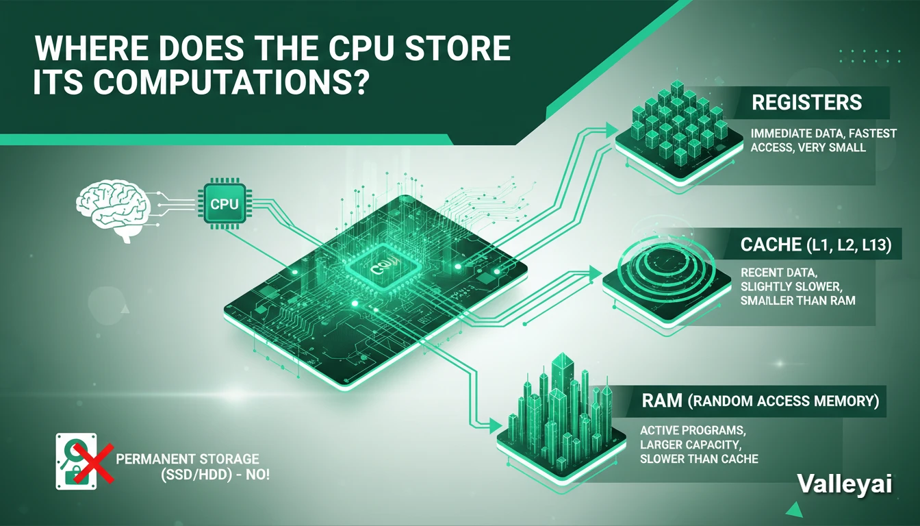
2. Short-Term Buffering: The Cache Hierarchy (The Desk)
Once the CPU finishes a calculation in a Register, it usually needs to save that number for use a few microseconds later. Sending it all the way back to RAM takes too long roughly 100 nanoseconds, which is an eternity for a 4GHz processor.
Instead, the CPU moves the computation to its internal Cache.
Cache is static random-access memory (SRAM) embedded directly on the processor chip. It acts as a staging area. The CPU guesses which data you will need next and keeps it close by.
This system is organized by proximity to the core:
- L1 Cache: The smallest and fastest layer. It stores data the CPU is likely to use immediately. It usually takes only 3 or 4 CPU cycles to access L1.
- L2 Cache: Slightly larger but slightly slower (around 10-12 cycles). If the data isn’t in L1, the CPU checks here.
- L3 Cache: The largest shared pool of memory on the chip. It allows different cores to share data without talking to the slow system RAM.
The Cache Miss Penalty:
Understanding cache is vital to understanding CPU performance. If the CPU looks for a computation result in L1, L2, and L3 and cannot find it (a Cache Miss), it has to stop working and wait for the data to be fetched from the main RAM. This stall creates noticeable latency in high-performance computing.
3. The Write-Back Policy: Why RAM is often outdated
A common misconception is that when a CPU changes a number, it immediately updates the RAM. In modern systems, this is rarely true.
CPUs typically use a Write-Back policy. When the CPU modifies data, it updates the value in its internal Cache and marks that specific line of memory as Dirty.
The data sitting in your main System RAM is now technically old. The CPU holds the only correct version of that computation in its cache. It will only write that Dirty data back to the System RAM when it absolutely has to usually when it needs to clear space in the cache for new tasks. This lazy approach prevents the pathways between the CPU and RAM (the memory bus) from being clogged with constant, tiny updates.
4. The Waiting Room: System RAM
System RAM (DRAM) is where computations go when the CPU is done with them for the moment, but the program is still running.
While we think of RAM as fast, to a CPU, it is incredibly distant. The latency is high because the electrical signals have to leave the CPU die, travel across the motherboard trace wires, enter the RAM stick, locate the data, and send it all the way back.
For this reason, the CPU never strictly computes in RAM. RAM is simply a holding pattern a warehouse where data sits until the CPU is ready to load it into the Registers/Cache to actually work on it.
5. Cold Storage: SSD / Hard Drive
Finally, we have the hard drive (SSD/HDD). It is crucial to understand that the CPU cannot execute code or compute data stored here.
The drive is strictly for non-volatile storage. If you want to run a program or edit a file saved on your SSD, the computer must first copy that data into RAM, then into the CPU Cache, and finally into the Registers. The lifecycle of a computation flows vertically through this chain; the CPU cannot skip steps.
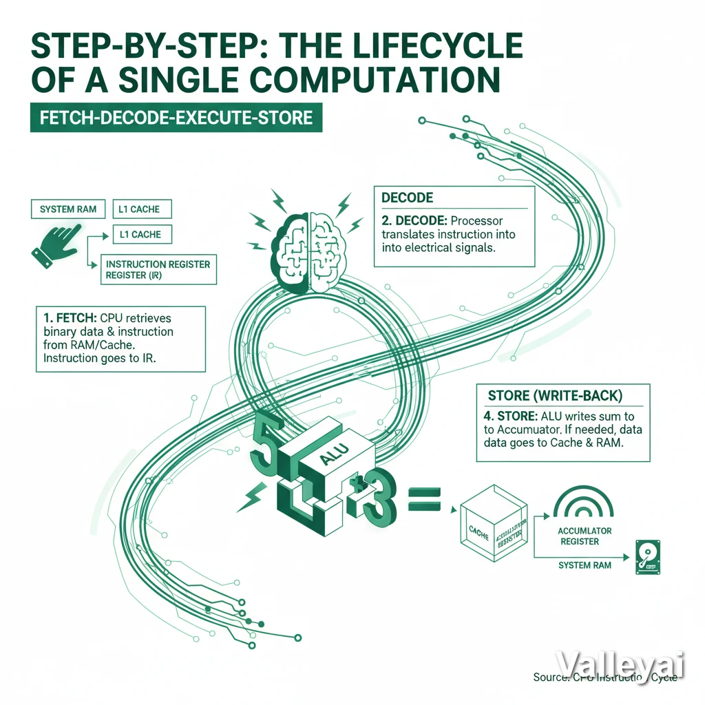
Step-by-Step: The Lifecycle of a Single Computation
The instruction cycle dictates exactly how a processor handles data. When a computer performs a basic operation such as adding two numbers together the CPU follows a strict, four-step workflow known as the Fetch-Decode-Execute-Store cycle.
Here is the exact journey of data during a computation:
- Fetch: The CPU Control Unit retrieves the binary data and the instruction (e.g., “Add these numbers”) from the system RAM or L1 Cache, placing the instruction into the Instruction Register (IR).
- Decode: The processor translates the instruction into physical electrical signals that the ALU can understand.
- Execute: The Arithmetic Logic Unit (ALU) performs the physical addition of the two numbers.
- Store (Write-Back): The ALU outputs the final sum and writes the computed data directly into the Accumulator Register. If the software requires that sum to be saved permanently, the CPU will then push the data down the hierarchy from the Register, through the Cache, and back into the system RAM.
Summary: The Latency Ladder
To visualize why the CPU fights so hard to keep computations in Registers and Cache, look at the cost of fetching data from each location (measured in clock cycles):
| Location | Distance from Core | Access Cost (Cycles) | Role |
|---|---|---|---|
| Registers | Zero (Inside Core) | < 1 Cycle | Immediate Processing |
| L1 Cache | On Die (Private) | ~4 Cycles | Immediate Reuse |
| L2 Cache | On Die (Private) | ~10 Cycles | Short-term Buffer |
| L3 Cache | On Die (Shared) | ~40-50 Cycles | Core Synchronization |
| System RAM | On Motherboard | ~100+ Cycles | Application State |
| SSD | SATA/NVMe Bus | Millions of Cycles | Permanent Storage |
The CPU stores its computations as close to the top of this list as physically possible. It only demotes data to lower tiers when it runs out of space. This extreme latency curve explains the entire architectural design of a modern processor. Computations must stay at the top of the ladder to maintain performance.
Architect’s Note: Latency metrics vary by specific hardware generation. Benchmarking tools like AIDA64 consistently demonstrate that retrieving a computation from RAM takes nearly 100 times longer than pulling it from an internal register.
The Assembly Perspective:
In x86 assembly language, a programmer might write ADD EAX, EBX. This command literally tells the processor: Take the computation stored in register EBX, add it to the computation stored in register EAX, and store the final result back into the EAX register.
Read also: The history of CPU
FAQs:
Which part of the CPU stores results of calculations?
The results of calculations are typically stored in registers within the CPU. Registers are small, high-speed storage locations that provide temporary storage for intermediate results during computations.
How Does the CPU Utilize Its Internal Storage During Computations?
The CPU utilizes its internal storage, such as registers and cache memory, to store intermediate results during computations. By storing intermediate results in internal storage, the CPU can quickly access and manipulate the data as needed.
Can the CPU Store Permanent Data?
No, the CPU cannot store permanent data. The CPU’s storage solutions, such as registers and cache memory, are volatile and lose their data when the computer is powered off. Permanent data is typically stored in secondary storage devices, such as hard disk drives.
What Is the Difference Between Cache and Registers?
The main difference between cache and registers is their size and access speed. Registers are small, high-speed storage locations within the CPU, while cache memory is larger and slightly slower. Registers provide immediate access to frequently used data, while cache memory stores recently accessed data for faster retrieval.
What role does the cache memory play in storing CPU computations?
Cache memory plays a crucial role in storing CPU computations by providing a fast storage solution for recently accessed data and instructions. It acts as a temporary storage location that enables the CPU to retrieve frequently used data quickly, improving overall system performance.
Where Does the CPU Store Its Computations?
The CPU stores its computations in both registers and cache memory.
What is the Fetch-Execute cycle?
The Fetch-Execute cycle is the fundamental process a CPU uses to operate. It fetches an instruction from memory, decodes what mathematical operation is required, executes the calculation in the ALU, and stores the resulting computation back into a register.
What is the difference between CPU registers and cache?
Registers are microscopic memory locations inside the CPU core used to hold the exact data being processed at that exact millisecond. Cache is a slightly larger, slower staging area on the CPU chip that buffers upcoming data from the System RAM.
Kaleem
My name is Kaleem and i am a computer science graduate with 5+ years of experience in Computer science, AI, tech, and web innovation. I founded ValleyAI.net to simplify AI, internet, and computer topics also focus on building useful utility tools. My clear, hands-on content is trusted by 5K+ monthly readers worldwide.