
Most computers built before 1960 couldn’t fit in a building lobby. Not because engineers lacked ambition but because the technology they were using made miniaturization physically impossible. The invention that broke that barrier wasn’t a single dramatic moment. It was a quiet September afternoon in 1958, inside a Texas Instruments lab, when Jack Kilby demonstrated something that would redefine every piece of computing hardware that followed.
What Do Most SERP Results Get Wrong About Computer Miniaturization?
The integrated circuit commonly called the microchip is the invention that allowed computers to become smaller in size.
Jack Kilby at Texas Instruments and Robert Noyce at Fairchild Semiconductor both independently developed functional integrated circuits in 1958. Kilby demonstrated his first in September; Noyce’s design, completed months later, proved more practical for mass production. Both contributions were essential. Neither can be fully credited without the other.
But here’s where most explanations go sideways: they say transistor when they mean integrated circuit, or they say microchip when they mean microprocessor. These are not interchangeable terms. Each describes a distinct invention solving a different problem.
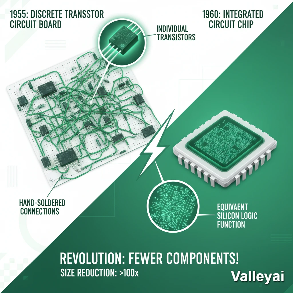
The transistor (invented at Bell Labs in 1947) replaced vacuum tubes and made circuits smaller and more efficient. That was real progress. But a transistor alone is a single switch. To build a functional computer circuit, you still needed to connect hundreds or thousands of them by hand with wires, solder joints, and individual components mounted on boards. That process was slow, expensive, and prone to failure.
The integrated circuit solved this by placing thousands of transistors, resistors, and capacitors onto a single piece of silicon all their connections formed simultaneously during manufacturing. No hand-wiring. No individual components to solder. One chip replaced an entire circuit board.
That’s the invention that made computers small.
The integrated circuit (IC), invented independently by Jack Kilby (Texas Instruments) and Robert Noyce (Fairchild Semiconductor) in 1958, enabled computer miniaturization by combining multiple electronic components transistors, resistors, and capacitors onto a single piece of silicon. This eliminated the need for hand-assembled discrete component circuits, dramatically reducing size, cost, and failure rates.
Why Was Computer Size a Hard Physical Limit Before the Microchip?
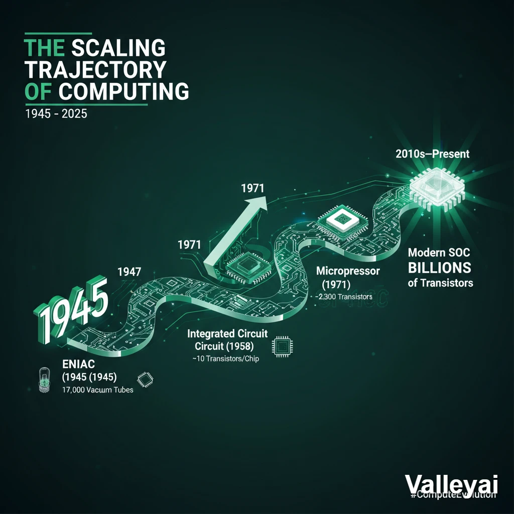
ENIAC one of the first general-purpose electronic computers, built at the University of Pennsylvania in 1945 occupied 1,800 square feet, weighed 30 tons, and consumed 150 kilowatts of power. It contained roughly 18,000 vacuum tubes.
Read also: ENIAC specs University of Pennsylvania archives
Those vacuum tubes weren’t just large. They generated enormous heat. Each one functioned like a small light bulb glass envelope, heated filament, controlled electron flow. Cooling ENIAC required industrial air conditioning infrastructure. And the tubes burned out regularly. With 18,000 of them running simultaneously, failures were almost constant. Technicians spent as much time replacing failed tubes as they did running computations.
Room-sized computers weren’t just impractical they were single-purpose machines. Moving them required industrial equipment. Reprogramming them took teams of engineers working for days. The economics of computing made it a government and military tool exclusively.
When Bell Labs’ William Shockley, John Bardeen, and Walter Brattain invented the transistor in 1947, things shifted. Transistors performed the same function as vacuum tubes controlling electrical signals but were solid-state. No glass envelope. No heated filament. Dramatically less heat. A fraction of the size.
Computers built with transistors shrank from room-sized to cabinet-sized. That was significant. But transistor-based computers still required engineers to wire together hundreds of discrete components by hand. Every connection was a potential failure point. Every solder joint was a liability.
The transistor solved the heat problem. It didn’t solve the assembly problem.
How Did the Integrated Circuit Replace an Entire Circuit Board?
The integrated circuit works by building an entire circuit transistors, resistors, capacitors, and all their interconnections directly into a thin slice of silicon during the manufacturing process itself.
Here’s the key mechanism: photolithography. A circuit pattern is projected onto a silicon wafer coated with light-sensitive material, much like exposing photographic film. Where light hits, the material changes. Chemical processes then etch away specific regions, deposit conductive materials, and implant atoms that alter silicon’s electrical properties. Repeat this process dozens of times with different patterns, and you’ve built an entire circuit not assembled it, built it at the microscopic level.
When you’re designing circuits with discrete transistors, every connection point is a potential failure. Each solder joint, each wire, each contact adds risk. The integrated circuit eliminated most of those failure points by forming all connections simultaneously in silicon. A chip with 1,000 transistors doesn’t have 1,000 separate components to fail it has one chip.
Silicon specifically made this possible at scale. Earlier transistors used germanium, but germanium becomes unstable at higher temperatures. Silicon’s native oxide layer silicon dioxide, or SiO₂ is thermally stable and acts as a natural insulator, enabling the gate structures that modern transistors require. Silicon was also abundant and relatively cheap to purify. Germanium was neither.
The result: circuits that previously required an entire printed circuit board could now fit on a chip smaller than a fingernail. And because photolithography could project ever-finer patterns using shorter wavelengths of light, the circuits could be made smaller with each manufacturing generation without redesigning the underlying logic.
That’s why the integrated circuit didn’t just enable one generation of smaller computers. It enabled continuous miniaturization.
The integrated circuit uses photolithography to etch complete circuits including transistors, resistors, and their connections directly into silicon during manufacturing. This process eliminates hand-assembled wiring, reduces failure points, and enables mass production of
complex circuits at microscopic scale. Silicon’s thermal stability and native oxide layer made it the preferred semiconductor material for IC manufacturing over germanium.
What Was the Invention Chain From Vacuum Tubes to Modern Chips?
| Year | Invention / Milestone | Key Figure(s) | Organization | Impact on Size |
|---|---|---|---|---|
| 1945 | ENIAC — first general-purpose computer | Eckert & Mauchly | University of Pennsylvania | 1,800 sq ft; 18,000 vacuum tubes |
| 1947 | Transistor invented | Shockley, Bardeen, Brattain | Bell Labs | Replaced vacuum tubes; cabinet-sized computers possible |
| 1958 | Integrated Circuit developed | Jack Kilby | Texas Instruments | Entire circuits on single silicon chip; book-sized computers possible |
| 1958–59 | Practical IC design for mass production | Robert Noyce | Fairchild Semiconductor | Enabled commercial IC manufacturing |
| 1965 | Moore’s Law formulated | Gordon Moore | Fairchild Semiconductor | Predicted transistor density doubling every ~2 years |
| 1971 | First commercial microprocessor (Intel 4004) | Ted Hoff, Federico Faggin | Intel | Entire CPU on one chip; desktop computers possible |
| 1980s–90s | VLSI (Very Large Scale Integration) | Industry-wide | Multiple | Millions of transistors per chip; laptops and mobile devices possible |
| 2010s–present | System-on-Chip (SoC) | Multiple (Apple, Qualcomm, Samsung) | Multiple | Billions of transistors; smartphone processors |
The transistor was necessary but not sufficient. The integrated circuit was the actual inflection point. Without it, transistor-based computers would have remained large, expensive, and hand-assembled indefinitely.
Gordon Moore’s 1965 observation that the number of transistors on a chip doubles approximately every 18 to 24 months only became meaningful because the integrated circuit gave manufacturers a scalable manufacturing process. Moore’s Law isn’t a law of physics. It’s a description of what photolithographic manufacturing made economically achievable, generation after generation.
Read also: Moore’s Law — Gordon Moore’s original 1965 Electronics Magazine paper
Why Does the 1958 Integrated Circuit Still Govern Every Device Today?
Modern smartphone processors contain between 15 and 20 billion transistors. If those transistors were individual components connected by hand-soldered wires, the phone would be the size of a refrigerator and it would fail constantly due to connection failures. The integrated circuit didn’t just enable miniaturization. It enabled reliability at scale.
The iPhone’s A-series chips, Qualcomm’s Snapdragon processors, and Apple Silicon’s M-series chips are all direct descendants of the 1958 integrated circuit. They’re built using the same fundamental principle photolithographic etching of circuits into silicon with the patterns now measured in nanometers rather than millimeters.
Current leading-edge chips are manufactured at 3nm and 2nm process nodes. That’s roughly the width of 10–15 silicon atoms. The physics of further scaling is genuinely approaching hard limits quantum tunneling effects become significant below 1nm but the architectural principle hasn’t changed since Kilby’s first demonstration.
Moore’s Law is slowing. The industry knows it. But the integrated circuit’s fundamental architecture integrating complete circuits into silicon during manufacturing remains the dominant computing paradigm more than 65 years after its invention.
Modern computing devices from smartphones to data center servers rely on
integrated circuits manufactured using photolithographic processes descended directly from the 1958 invention. Current chips contain billions of transistors at process nodes measured in nanometers. Despite approaching physical scaling limits, the integrated circuit remains the foundational architecture of all contemporary computing hardware.
The Terminology Trap That Confuses Almost Everyone
Three terms appear constantly in discussions about computer miniaturization. They’re often used interchangeably. They shouldn’t be.
Transistor: A single electronic switch that controls the flow of electrical current. The transistor
replaced vacuum tubes. One transistor = one switch. Invented 1947.
Integrated Circuit (Microchip): A complete circuit containing thousands (later millions, then
billions) of transistors, resistors, and capacitors plus all their interconnections built onto a
single piece of silicon. The integrated circuit is what made computers small. Invented 1958.
Microprocessor: A specific type of integrated circuit that contains a complete central processing unit (CPU). All microprocessors are integrated circuits. Not all integrated circuits are microprocessors. The first commercial microprocessor (Intel 4004) appeared in 1971, 13 years after the IC.
A common misunderstanding: The microchip is just a smaller transistor. It isn’t. The microchip is thousands of transistors plus all the connections between them, manufactured as a single unit on silicon.
The breakthrough wasn’t making individual transistors smaller it was integrating them together
reliably, eliminating the hand-assembly problem that had kept transistor computers large and expensive.
The distinction between transistor and IC is precisely why the question “which invention allowed computers to become smaller in size?” has a specific correct answer. The transistor was necessary. The integrated circuit was sufficient.
Most guides get this wrong by treating the transistor as the primary answer. The transistor made computers smaller. The integrated circuit made them small enough to be useful, affordable, and eventually pocket-sized.
A transistor is a single electronic switch; an integrated circuit (IC) combines thousands of transistors and their connections onto one silicon chip; a microprocessor is a specific IC containing a complete CPU. The IC not the transistor alone enabled computer miniaturization by eliminating hand-assembled wiring. All three terms are distinct technologies, though they are frequently and incorrectly used interchangeably.
Frequently Asked Questions
What is the invention that allowed computers to become smaller?
The integrated circuit, invented in 1958 by Jack Kilby at Texas Instruments and independently by Robert Noyce at Fairchild Semiconductor. The integrated circuit placed thousands of electronic components onto a single silicon chip, eliminating the need for hand-assembled discrete component circuits and enabling dramatic size reduction.
Who invented the microchip?
Jack Kilby and Robert Noyce both independently developed integrated circuits in 1958. Kilby’s design (September 1958) is often cited as the first demonstration; Noyce’s design proved more practical for mass production. Both are recognized as co-inventors of the integrated circuit. Kilby received the Nobel Prize in Physics in 2000 for his contribution.
What came before the integrated circuit?
The transistor (1947, Bell Labs) preceded the integrated circuit and replaced vacuum tubes. Before transistors, computers used vacuum tubes glass-enclosed devices that generated enormous heat and failed frequently. Transistors made computers smaller and more reliable, but circuits still required hand assembly. The integrated circuit eliminated that assembly requirement
What is the difference between a transistor and a microchip?
A transistor is a single electronic switch. A microchip (integrated circuit) contains thousands to billions of transistors plus resistors, capacitors, and all their connections built onto one silicon chip during manufacturing. The microchip integrates what previously required an entire hand-assembled circuit board.
How small can computer chips get?
Current leading-edge chips are manufactured at 3nm and 2nm process nodes roughly 10–15 silicon atoms wide. Quantum tunneling effects begin to interfere with transistor function below approximately 1nm, representing a near-term physical limit. The industry is exploring 3D chip stacking, new materials (gallium nitride, carbon nanotubes), and alternative architectures to continue performance scaling beyond traditional photolithographic limits.
Why were early computers so large?
Early computers like ENIAC (1945) used vacuum tubes approximately 18,000 of them which were physically large, generated significant heat requiring industrial cooling, and failed regularly. Even after transistors replaced vacuum tubes, computers remained large because circuits required hand- assembling hundreds of discrete components. The integrated circuit eliminated the hand-assembly requirement, enabling true miniaturization.
The integrated circuit didn’t just change how computers were built. It changed who could use them, where they could go, and what they could become. Every device in your pocket, on your desk, or embedded in your car traces its physical form back to a September afternoon in 1958 when Jack Kilby proved that an entire circuit could live on a chip of silicon smaller than a paperclip.
The next time someone asks what made computers small, the honest answer isn’t “the transistor” or “the microchip” as a vague term. It’s the integrated circuit a specific invention, by specific people, solving a specific problem that transistors alone couldn’t crack. That precision matters, because understanding why it worked is what tells you why modern computing looks the way it does.
Related Topics For More Learning
- What is Moore’s Law? Understanding the rate of chip scaling.
- Analog vs. Digital Computers: How the method of calculation changed hardware needs.
- The History of the CPU: From the Intel 4004 to modern multi-core processors.
Kaleem
My name is Kaleem and i am a computer science graduate with 5+ years of experience in Computer science, AI, tech, and web innovation. I founded ValleyAI.net to simplify AI, internet, and computer topics also focus on building useful utility tools. My clear, hands-on content is trusted by 5K+ monthly readers worldwide.