The history of the Central Processing Unit (CPU) is often presented as a simple timeline of numbers getting bigger: clock speeds rising, transistor counts doubling, and prices falling. But looking at processor history this way misses the actual story.
The evolution of the CPU is actually a history of engineers hitting brick walls limitations in memory, physics, and heat and having to fundamentally reinvent how a computer thinks to get around them. We didn’t get from the Intel 4004 to the Core i9 simply by shrinking transistors; we got there by changing the rules of the game every time physics tried to stop us.
Here is the history of the CPU, viewed through the eras of the architectural problems that defined them.
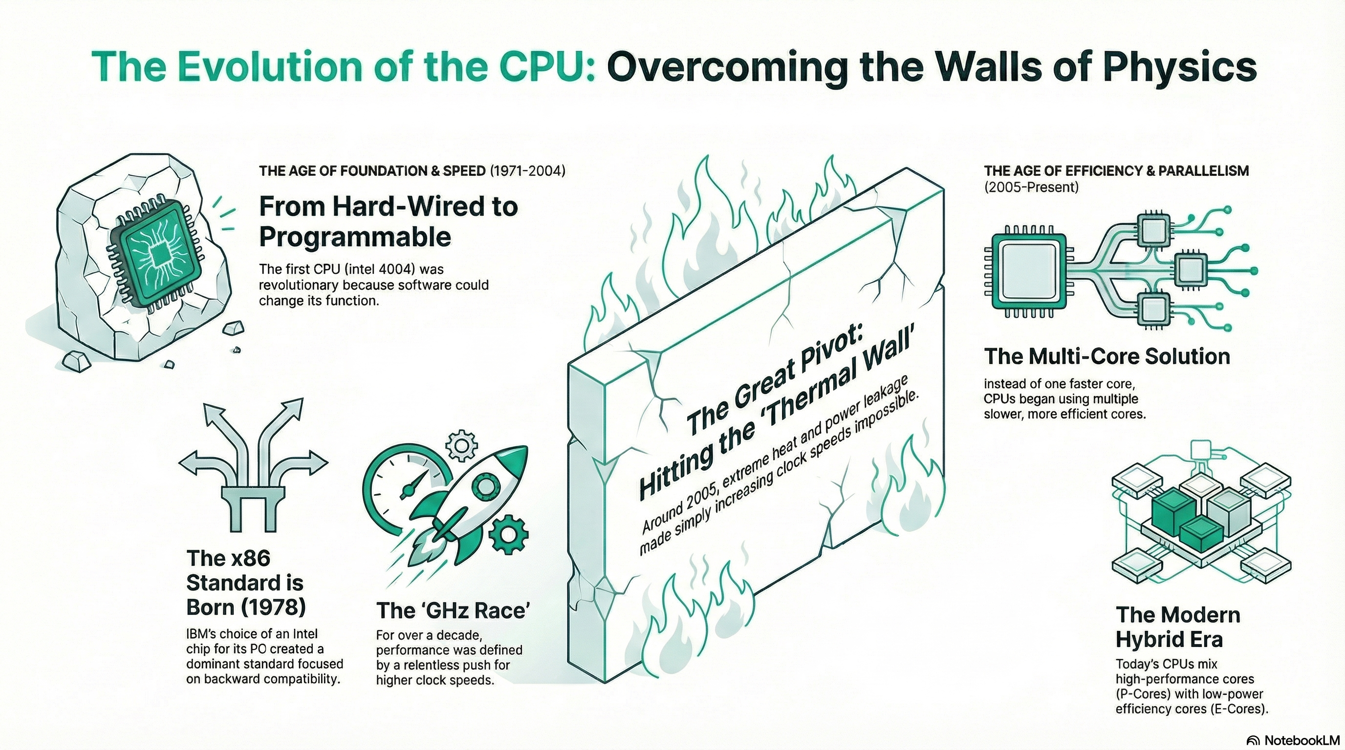
I. The Era of Integration: Getting the Math on the Silicon (1971–1978)
In the early 1970s, the challenge wasn’t speed; it was geography. Computers were room-sized behemoths because the logic gates required to perform calculations were spread across thousands of discrete components.
The Intel 4004: The Accidental Generalist
When Intel released the 4004 in 1971, they weren’t trying to invent the personal computer. They were fulfilling a contract for a Japanese calculator company, Busicom. The genius of the 4004 wasn’t its power—it could only handle 4 bits of data at a time and ran at a sluggish 740 kHz—but its programmability.
Prior to this, logic was hard-wired. If you wanted a calculator, you wired circuits to do math. If you wanted a controller for a traffic light, you wired circuits to time lights. The 4004 introduced the concept of the General Purpose processor. The hardware remained static, but the software could change the function. This is the foundational concept of all modern computing: hardware is the canvas; software is the paint.
The Shift to 8-Bit
The 4004 was sufficient for numbers, but the industry quickly hit a bottleneck: text. Standard text encoding (ASCII) requires 7 to 8 bits per character. A 4-bit chip had to cycle twice just to understand a single letter A.
The Intel 8008 and subsequently the 8080 (1974) moved to 8-bit architectures, allowing computers to handle data in chunks that made sense for human communication. This shift transformed the CPU from a calculator component into the brain of the first true hobbyist computers, like the Altair 8800.
For more knowledge read also : technological breakthrough for smaller computers
II. The Era of Standardization: The Birth of x86 (1978–1989)
By the late 70s, the problem was no longer can we build it? but can we run software on it? Every new computer architecture required software to be rewritten from scratch. The industry was fragmented and inefficient.
The 8086 and the IBM Choice
In 1978, Intel released the 8086, a 16-bit processor. It wasn’t necessarily the most technically advanced chip available, but it had one massive stroke of luck: IBM chose a variant of it (the 8088) for the original IBM PC.
Because the IBM PC became the dominant standard for business, the architecture of its processor x86 became the industry standard. This created the golden rule of modern CPU manufacturing: Backward Compatibility. A program written for an 8086 in 1978 can, theoretically, still be understood by a modern Intel Core processor today. This decision prioritized software legacy over architectural purity, a trade-off that still dictates how chips are designed.
The 386 and Protected Mode
While the 8086 started the standard, the Intel 386 (1985) defined the modern computing experience. It was a 32-bit chip, but its real contribution was Protected Mode.
Before the 386, if a program crashed, it took the whole computer down with it because every program had unrestricted access to system memory. Protected Mode allowed the CPU to create virtual sandboxes for applications. This hardware feature is what made modern operating systems like Windows 95, Linux, and OS X possible. It allowed for true multitasking running a spreadsheet and a word processor simultaneously without them overwriting each other’s memory.
III. The Era of Speed & Efficiency: The GHz Race (1990–2004)
Once the 32-bit standard was set, the focus shifted entirely to performance. For nearly 15 years, the marketing message was simple: More MHz = Better. But underneath the heat spreaders, engineers were using clever tricks to make chips faster than their clock speeds suggested.
The Assembly Line: Pipelining
To get more speed, engineers introduced Pipelining. Imagine a laundry process: wash, dry, fold.
- Non-pipelined: You wash, wait, dry, wait, fold, wait. Then start the next load.
- Pipelined: As soon as load 1 moves to the dryer, load 2 goes into the washer.
Processors like the original Pentium broke instructions down into smaller stages, allowing different parts of the CPU to work on different instructions simultaneously.
Out-of-Order Execution
The next bottleneck was inefficiency. Sometimes the CPU would sit idle waiting for data from the slow system memory. To fix this, engineers introduced Out-of-Order Execution (notably in the Pentium Pro).
If the CPU was waiting for data to complete Instruction A, but Instruction B was ready to go and didn’t depend on A, the CPU would skip ahead, do B, and come back to A later. This transformed the CPU from a linear worker into a dynamic project manager, drastically increasing Instructions Per Clock (IPC).
AMD Forces the 64-Bit Issue
During this era, Intel’s competitor AMD stopped being a budget clone manufacturer and became an innovator. In 2003, AMD released the Athlon 64.
Intel was trying to push a new, non-compatible 64-bit architecture (Itanium) that required rewriting software. AMD took a different approach: they extended the standard x86 architecture to 64-bit (x86-64). It could run old 32-bit Windows perfectly while offering 64-bit power. The market voted with its wallet, and Intel was forced to license AMD’s technology. This is why your modern Intel chip technically uses an AMD64 instruction set.
IV. The Great Pivot: The Thermal Wall (2005)
Around 2004, the Free Lunch of simply increasing clock speeds ended abruptly. Intel had projected its NetBurst architecture (used in the Pentium 4) would eventually hit 10 GHz. Instead, it hit a wall of physics.
The Power Wall
As transistors got smaller and clock speeds pushed past 3 GHz, heat density became unmanageable. The chips were leaking so much electricity that cooling them required impractical amounts of energy and massive heatsinks. The Pentium 4 Prescott ran so hot it was notoriously dubbed the Pres-hot.
Engineers realized that pushing frequency further would result in chips that melted before they calculated. The era of single-core frequency scaling was dead.
V. The Multi-Core Era: Parallelism (2006–Present)
If you can’t build a faster engine, you build a car with two engines. This was the logic behind the Intel Core 2 Duo and the AMD Athlon 64 X2.
The Shift to Wide Architectures
Intel abandoned the NetBurst architecture and looked back at their mobile chips (Pentium M), which were designed for efficiency, not raw speed. They widened the pipeline to do more work per cycle at lower clock speeds. This marked the transition from “Deep and Fast” to “Wide and Efficient.”
The Software Catch-Up (Amdahl’s Law)
The challenge with multi-core CPUs wasn’t hardware; it was software. A 3 GHz single-core chip runs one task at 3 GHz. A dual-core 1.5 GHz chip has the same total theoretical power, but only if the software can be split into two equal pieces.
This introduced users to Amdahl’s Law, which dictates that the speedup of a program is limited by the portion of it that cannot be parallelized. For years, gamers saw little benefit from Quad-Core chips because games relied heavily on a single main thread. It took nearly a decade for software developers to effectively utilize 4, 8, and 16 cores.
VI. The Modern Era: Heterogeneity and Chiplets (2017–Present)
Today, we are facing a new bottleneck: Moore’s Law (the doubling of transistors) is slowing down and becoming prohibitively expensive.
The Chiplet Revolution
AMD solved the cost problem with the Ryzen architecture. Instead of trying to print one massive, perfect CPU (which is difficult and yields many defects), they started printing smaller chiplets and gluing them together on a single package. This allowed them to easily scale from 6 cores to 64 cores (Threadripper) simply by adding more chiplet bricks, disrupting Intel’s dominance in the high-end market.
Hybrid Architectures (Big.LITTLE)
The most recent shift, popularized by ARM in mobile phones and adopted by Intel in its 12th Gen (Alder Lake) chips, is Heterogeneous Computing.
Modern CPUs now combine two types of cores:
- Performance Cores (P-Cores): Big, power-hungry cores for gaming and rendering.
- Efficiency Cores (E-Cores): Small, low-power cores for background tasks like email syncing or Windows updates.
This design acknowledges that not all math requires a supercomputer. By offloading background noise to E-cores, the P-cores are free to boost higher for heavy workloads without overheating the entire package.
Conclusion: The End of General Purpose?
We have moved from the 4004, a 4-bit chip designed to run a calculator, to hybrid processors that contain specialized neural engines for AI, dedicated media encoders for streaming, and distinct cores for efficiency.
The future of the CPU is likely less about the Central Processing Unit doing everything and more about it acting as a conductor orchestrating a symphony of specialized accelerators (GPUs, NPUs, TPUs) to bypass the physical limits of silicon.
Recommended Next Steps For More Learning
- Understanding Architecture: Learn the difference between RISC (ARM/Apple Silicon) and CISC (x86 Intel/AMD) to understand why battery life differs so much between devices.
- The Nanometer Race: Research what 3nm or 5nm manufacturing nodes actually mean (hint: it’s no longer the actual size of the gate).
- Bottlenecks: Investigate how Memory Bandwidth (DDR4 vs DDR5) impacts CPU performance in modern systems.
Kaleem
My name is Kaleem and i am a computer science graduate with 5+ years of experience in Computer science, AI, tech, and web innovation. I founded ValleyAI.net to simplify AI, internet, and computer topics also focus on building useful utility tools. My clear, hands-on content is trusted by 5K+ monthly readers worldwide.