
The four basic logic gates are AND, OR, XOR (Exclusive-OR), and NOT. They are the fundamental building blocks of digital electronics, taking one or more binary inputs (0s and 1s) to produce a single logical output based on the rules of Boolean algebra. Understanding these gates fundamentally requires observing how they govern electronic switching circuits in the physical world.
While most tutorials stop at abstract truth tables, mastering digital design requires connecting theoretical mathematics to physical hardware. This ultimate guide bridges the gap between the foundational Boolean algebra developed by George Boole and Claude Shannon, and modern, physical applications. Today, logic gates serve as the microscopic decision-makers inside everything from basic calculators to high-performance FPGAs (Field Programmable Gate Arrays).
We will explore how these gates function, how to wire them on a breadboard using 7400-series Integrated Circuits (ICs), and how to map them directly into Python bitwise operators and Verilog.
Logic gates are the physical mechanisms that process the fundamental binary machine language of 0s and 1s into complex decisions and calculations.
Introduction to Digital Logic: Understanding High/Low States
Digital logic is the foundation of modern computing, operating on binary signals represented as either a “High” (1) or “Low” (0) state. These states correspond to specific voltage levels within hardware components like MOSFETs, determining how digital circuits process, store, and transmit information.
In physical hardware, these 1s and 0s are not just abstract numbers; they are distinct electrical voltage levels.
- TTL (Transistor-Transistor Logic): Typically, a Low is 0V to 0.8V, and a High is 2.2V to 5V.
- CMOS (Complementary Metal-Oxide-Semiconductor): Uses closer to 0V for Low and 3.3V/5V for High, offering lower power consumption and higher noise immunity.
Understanding these thresholds is critical when designing CPU architecture logic gate mapping or performing electronic circuit troubleshooting.
How Do Logic Gates Work in Real Life?
In real life, logic gates work by acting as microscopic, electronically controlled switches. Inside modern microchips, these switches are made of transistors specifically MOSFETs in CMOS circuits or bipolar junction transistors in TTL (Transistor-Transistor Logic). When voltage is applied to an input, the transistor opens or closes, allowing current to flow to the output.
To understand the core mechanics without needing a degree in silicon fabrication, we can translate these microscopic electronic switching circuits into highly visible mechanical and water flow analogies.
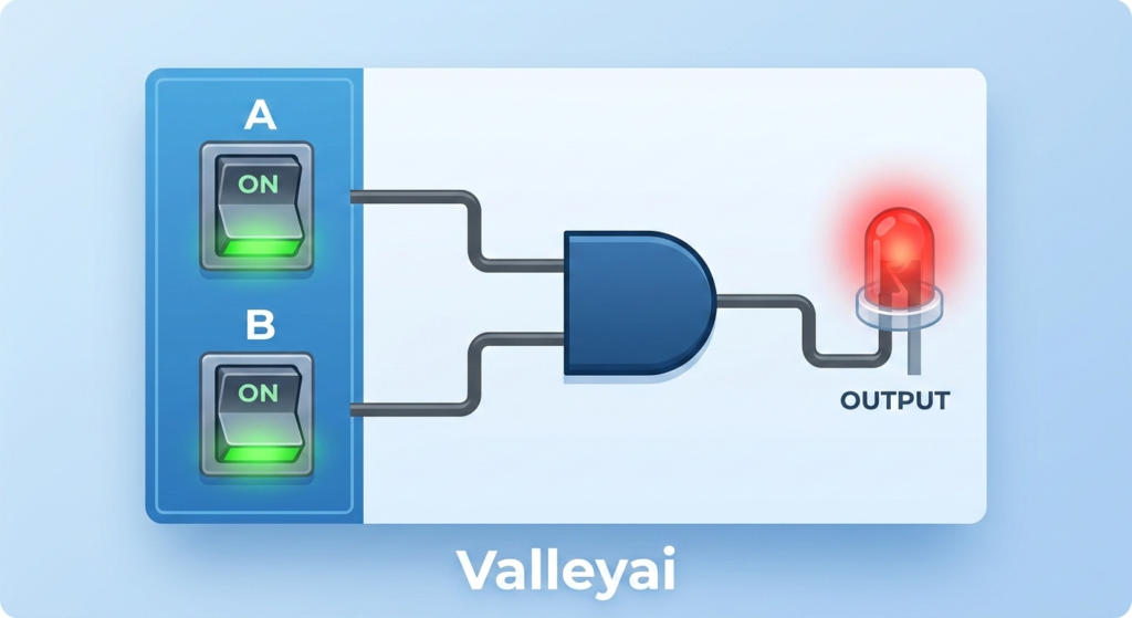
The AND Gate: Logical Multiplication, Truth Table, and Schematic Symbols
The AND gate outputs a High (1) signal only if all its inputs are High (1). If any input is Low (0), the output remains Low. In Boolean algebra, this is represented as logical multiplication (A · B = Y), and it is used to ensure multiple conditions are met simultaneously.
Symbol: A D-shaped symbol where the straight edge represents the inputs and the curved edge leads to the output.
Boolean Expression: $Y = A \cdot B$
AND Gate Truth Table
| Input A | Input B | Output Y |
|---|---|---|
| 0 | 0 | 0 |
| 0 | 1 | 0 |
| 1 | 0 | 0 |
| 1 | 1 | 1 |
Code & Hardware Equivalents:
- Python Bitwise Operator:
result = a & b - Verilog:
assign Y = A & B; - IC Pinout Diagram Reference: The 74LS08 is a quad 2-input AND gate IC. Pins 1 and 2 are inputs for the first gate, and Pin 3 is the output.
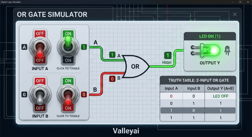
The OR Gate: Logical Addition, Truth Table, and Inclusive Logic Explained
The OR gate outputs a High (1) signal if at least one of its inputs is High (1). It only outputs a Low (0) when all inputs are Low. This represents logical addition in Boolean algebra (A + B = Y), functioning as an inclusive “either/or/both” decision block.
Symbol: A shield-like shape with a curved input edge and a pointed output.
Boolean Expression: $Y = A + B$
OR Gate Truth Table
| Input A | Input B | Output Y |
|---|---|---|
| 0 | 0 | 0 |
| 0 | 1 | 1 |
| 1 | 0 | 1 |
| 1 | 1 | 1 |
Code & Hardware Equivalents:
- Python Bitwise Operator:
result = a | b - Verilog:
assign Y = A | B; - IC Pinout Diagram Reference: The 74LS32 is a quad 2-input OR gate IC. Comparing the 74LS08 vs 74LS32 pin configuration, both share identical power/ground and input/output pin mapping, making them easy to swap on a breadboard.
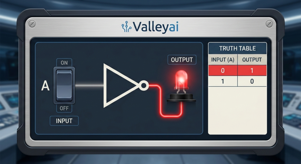
The NOT Gate (Inverter): Logic Reversal and Signal Phase Shifting
The NOT gate, or inverter, is a single-input gate that outputs the exact opposite of its input. If the input is High (1), the output is Low (0), and vice versa. It is primarily used for logic reversal and signal phase shifting in timing circuits.
Symbol: A triangle pointing to the right, with a small circle (bubble) at the output tip indicating inversion.
Boolean Expression: $Y = \overline{A}$
NOT Gate Truth Table
| Input A | Output Y |
|---|---|
| 0 | 1 |
| 1 | 0 |
Hardware Reference: The 74LS04 is a hex inverter IC, containing six independent NOT gates.
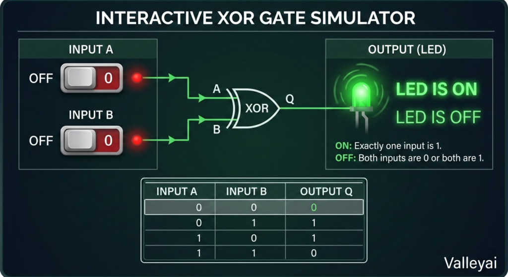
The XOR Gate: Exclusive-OR Mechanics and Bitwise Parity
The XOR (Exclusive-OR) gate outputs a High (1) signal only when its inputs are different from each other. If both inputs are the same (both High or both Low), the output is Low (0). It is essential for bitwise parity checking and arithmetic operations.
Symbol: Similar to an OR gate, but with an additional curved line curving across the inputs.
Boolean Expression: $Y = A \oplus B$
XOR Gate Truth Table
| Input A | Input B | Output Y |
|---|---|---|
| 0 | 0 | 0 |
| 0 | 1 | 1 |
| 1 | 0 | 1 |
| 1 | 1 | 0 |
What is the real-world application of an XOR gate?
XOR gates are the backbone of the Arithmetic Logic Unit (ALU) inside a CPU. They are used to build Half Adders and Full Adders to perform binary addition. Also, they are heavily utilized in cryptography and for generating parity bits to detect errors in data transmission.
Comparing Basic Gates: Summary Table of Boolean Expressions and Truth Table Outputs
Understanding the differences between digital logic fundamentals requires comparing their outputs side-by-side. The following summary table provides a quick reference for AND, OR, XOR, and NOT gates, displaying their Boolean expressions and combined truth table outputs.
| Inputs (A, B) | AND (A · B) | OR (A + B) | XOR (A ⊕ B) | NOT (Ā) |
|---|---|---|---|---|
| 0, 0 | 0 | 0 | 0 | 1 |
| 0, 1 | 0 | 1 | 1 | 1 |
| 1, 0 | 0 | 1 | 1 | 0 |
| 1, 1 | 1 | 1 | 0 | 0 |
Note: The NOT output in this table corresponds only to Input A.
Practical Applications: From Transistors to Integrated Circuits (ICs)
How do logic gates work in a modern CPU?
In a modern CPU architecture, billions of microscopic MOSFET transistors are wired together on a silicon die to form logic gates. These gates are clustered into functional blocks. For instance, combining XOR and AND gates creates arithmetic circuits in the ALU. Multiplexers (built from AND, OR, and NOT gates) route data buses. Hardware description languages like VHDL and Verilog are used to map these logic gates into a synthesized Register-Transfer Level (RTL) netlist before manufacturing.
How to Combine Logic Gates: A Brief Overview of Universal Gates (NAND/NOR)
Universal gates, specifically NAND and NOR, can be combined to replicate the function of any other basic logic gate (AND, OR, NOT, XOR). This drastically reduces manufacturing costs, as engineers can build entire complex digital circuits using only a single type of mass-produced gate.
By tying the inputs of a NAND gate together, it becomes a NOT gate. Inverting the output of a NAND gate gives you an AND gate. This universal property is heavily detailed in M. Morris Mano’s “Digital Design” and is an industry standard for optimizing physical space on silicon wafers.
Real-World Troubleshooting: Breadboards, ICs, and Floating Inputs
A common disconnect in learning digital logic is moving from the theoretical truth table to the physical breadboard. Here are real-world logic gate debugging scenarios.
Wiring Logic Gates on a Breadboard Tutorial
How do you connect a logic gate to a breadboard?
- Power and Ground: Place your 7400-series IC (e.g., 74LS08) across the center trench of the breadboard. Connect Pin 14 (VCC) to the 5V rail and Pin 7 (GND) to the ground rail.
- Inputs: Connect standard jumper wires or push-buttons to Pins 1 and 2.
- Pull-Down Resistors: Connect a 10kΩ pull-down resistor from each input pin to ground to prevent floating inputs (explained below).
- Outputs: Connect Pin 3 to a 220Ω current-limiting resistor, followed by an LED connected to ground.
How to Fix Floating Input Logic Errors
One of the most frequent issues in hardware-in-the-loop debugging is the “floating input.” If a CMOS or TTL input pin is left unconnected, it acts like an antenna, picking up ambient electromagnetic noise. This causes the gate to rapidly toggle between High and Low unpredictably.
The Fix: Always use pull-up or pull-down resistors to explicitly tie inputs to a known High (VCC) or Low (GND) state when a switch is open. You can verify a floating input by hooking up a logic analyzer or multimeter and watching the voltage erratically drift between 1.2V and 2.0V.
Testing Gate Integrity
How to test if a logic gate IC is working?
Using an oscilloscope or a logic analyzer, apply a known High/Low pulse sequence to the input pins and measure the output pin. Compare the resulting waveforms to the expected truth table. In high-speed circuits, you can also use an oscilloscope to measure the propagation delay (the time it takes for a signal to pass from input to output, usually measured in nanoseconds per Nexperia AN10898 guidelines).
(FAQs)
What is the difference between bitwise logic and boolean logic in coding?
In programming (like Python), Boolean logic (e.g., and, or, not) evaluates the truthiness of entire expressions and returns a single True or False. Bitwise logic (e.g., &, |, ^, ~) looks at the binary representation of integers and applies the physical logic gate operations parallelly across each individual bit.
What are the truth tables for AND, OR, and XOR?
Truth tables map all possible input combinations (1s and 0s) to their corresponding outputs. AND outputs 1 only when all inputs are 1. OR outputs 1 when any input is 1. XOR outputs 1 only when inputs are mismatched. (See the “Comparing Basic Gates” summary table above for visual reference).
What is the difference between OR and XOR?
The primary difference between OR and XOR (Exclusive-OR) is how they handle multiple true inputs. An OR gate outputs true if one or both inputs are true. An XOR gate is strictly exclusive; it outputs true only if the inputs are different from one another (one true, one false).
Why is XOR used in error detection and cryptography?
XOR is used in cryptography because it possesses a unique property of perfect reversibility without data loss. When you XOR plain text with a key, it scrambles it; XORing the scrambled text with the same key perfectly restores the plain text.
Sources: IEEE Standard 91/91a-1991, Texas Instruments Logic Guide, MIT OpenCourseWare (6.004)
Safety Disclaimer: Always handle 7400-series Integrated Circuits and CMOS components with proper ESD (Electrostatic Discharge) precautions. Observe maximum voltage limits (typically 5V for standard TTL) to avoid component damage.
Kaleem
My name is Kaleem and i am a computer science graduate with 5+ years of experience in Computer science, AI, tech, and web innovation. I founded ValleyAI.net to simplify AI, internet, and computer topics also focus on building useful utility tools. My clear, hands-on content is trusted by 5K+ monthly readers worldwide.