- Editorial Note: This article synthesizes data from TSMC roadmaps, IEEE research papers, and comparative die-shot analysis to explain the physical realities behind marketing nomenclature.
For the better part of a decade, nanometers (nm) have been the primary yardstick for technological progress. From smartphones to supercomputers, the race to zero suggests that smaller numbers automatically equal better devices. But as we transition from the established 5nm standard to the maturing 3nm landscape, the rules have changed.
We are hitting the limits of physics. The gap between 5nm and 3nm isn’t just about shrinking wires; it represents a fundamental architectural overhaul from how we build transistors to how we define measurements.
If you are holding a device running a 5nm chip (like the A15 or A16 Bionic) and wondering if the jump to a 3nm device (like the A17 Pro or Snapdragon 8 Gen 5) is worth the cost, this guide explains the engineering reality behind the hype.
Read also: historical inventions that enabled computer miniaturization
The Marketing Myth: The Node Gap Explained
Core Insight: 3nm describes a performance class, not a physical measurement.
Historically, the node name (e.g., 90nm, 45nm) referred to the gate length of the transistor the actual physical switch inside the chip. That correlation broke around 1997. Today, 3nm is a marketing term used by foundries like TSMC and Samsung Foundry to indicate an improvement over the previous generation.
If you were to measure a 3nm transistor under a transmission electron microscope, you wouldn’t find many features that measure exactly 3 nanometers.
The Real Measurements: Pitch vs. Label
To understand the actual density increase, we look at Fin Pitch (width between fins) and Contacted Poly Pitch (CPP).
| Marketing Node | Actual Gate Pitch (Approx.) | Metal Pitch (Approx.) | Transistor Density (MTr/mm²) |
|---|---|---|---|
| 7nm (N7) | 57nm | 40nm | ~91.2 |
| 5nm (N5) | 51nm | 30nm | ~138 |
| 3nm (N3) | 48nm | 22nm | ~220+ |
Analyst Note: While the physical features aren’t shrinking linearly, the transistor density (how many switches we can pack into a square millimeter) is nearly doubling. This density is what keeps Moore’s Law alive, allowing for more cache, better AI engines, and complex GPU cores on the same sized silicon wafer.
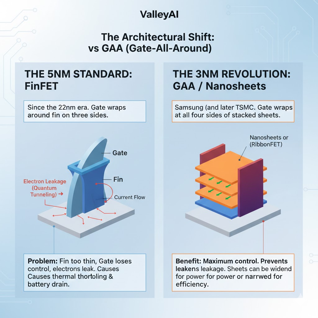
The Architectural Shift: FinFET vs. GAA (Gate-All-Around)
This is the most critical technical distinction that most mainstream reviews miss. The move from 5nm to 3nm (and beyond) forces a change in the physical shape of the transistor to prevent quantum tunneling a phenomenon where electrons leak through the switch even when it’s turned off, draining battery.
The 5nm Standard: FinFET
Since the 22nm era, the industry has used FinFET. Imagine a shark fin sticking up from the silicon. The gate wraps around the fin on three sides (left, right, top) to control the flow of electricity.
- The Problem: As we shrink to 3nm, the fin gets too thin. The Gate loses control, and electrons leak. This causes thermal throttling and battery drain.
The 3nm Revolution: GAA / Nanosheets
To fix this, Samsung (and later TSMC at 2nm) moved to Gate-All-Around (GAA), also known as RibbonFET or MBCFET.
- The Visual: Imagine a stack of three sheets of paper floating horizontally. The Gate material wraps around all four sides of these sheets.
- The Benefit: Maximum control. By wrapping the channel completely, the chip can cut off voltage leakage almost entirely. It also allows engineers to widen the sheets to push more power for high-performance tasks (gaming) or narrow them for efficiency (background tasks).
Visual Concept: A side-by-side diagram showing a FinFET (3-sided gate) leaking electrons vs. a GAA (4-sided gate) effectively trapping the current.
Technical Breakdown: 3nm vs 5nm Performance
What does this architectural shift yield in hard numbers? Based on TSMC N3 vs N5 process data and Samsung 3nm GAA whitepapers, here is the PPA (Power, Performance, Area) breakdown.
Power Efficiency (The Battery King)
- 3nm Advantage: At the same speed, a 3nm chip consumes roughly 30-35% less power than a 5nm chip.
- Why? The tighter lithography (enabled by ASML’s EUV machines) and reduced leakage mean the chip doesn’t have to work as hard to flip a switch.
Performance Speed (The Hz Race)
- 3nm Advantage: At the same power draw, 3nm offers a 10-15% speed increase.
- Reality Check: The raw speed gains are slowing down. The days of 50% jumps are over. The focus has shifted to efficiency.
Logic Density
- 3nm Advantage: 1.6x to 1.7x density improvement.
- Impact: This allows manufacturers (like Apple or NVIDIA) to double the size of the Neural Engine or GPU cores without making the phone or graphics card physically larger.
The Foundry Race: TSMC vs Samsung vs Intel
Not all 3nm chips are created equal. The manufacturing method matters as much as the node name.
TSMC (The Market Leader)
- Strategy: TSMC stuck with FinFET for their initial 3nm nodes (N3B, N3E) to ensure high yields (fewer defective chips per wafer). This is what powers the Apple A17 Pro and M3/M4 series.
- Pros: Reliable, massive volume capability.
- Cons: FinFET is pushed to its absolute physical limit here.
Samsung Foundry (The Innovator)
- Strategy: Samsung gambled by switching to GAA (MBCFET) early at 3nm.
- Pros: Better theoretical power efficiency and voltage control due to the new architecture.
- Cons: They faced significant yield challenges early on, making it harder to attract massive clients like Qualcomm initially.
Intel (The Comeback Kid)
- Strategy: Under IDM 2.0, Intel is racing to catch up with Intel 3 and Intel 18A. They are aggressively adopting High-NA EUV (the next generation of lithography lasers) to print smaller features than competitors.
Consumer Impact: Should You Upgrade?
Is 3nm worth the upgrade for gaming, battery life, or professional workflows? Use this decision matrix.
Scenario A: The Smartphone User
- Current Device: iPhone 13/14 (5nm/4nm) or Galaxy S22/S23.
- Verdict: Wait.
- Reasoning: While 3nm improves battery efficiency, the real-world battery life of phones hasn’t doubled because manufacturers are using the extra efficiency to power brighter screens (2000+ nits) and run hotter AI models. The 5nm chips are still incredibly capable for daily tasks.
Scenario B: The Mobile Gamer / Power User
- Current Device: 2+ years old.
- Verdict: Upgrade.
- Reasoning: 3nm chips like the Snapdragon 8 Elite Gen 5 or A17 Pro handle sustained loads much better. In thermal throttling tests (e.g., Genshin Impact or Ray Tracing benchmarks), 3nm chips maintain peak framerates for 20-30 minutes longer before dimming the screen or slowing down, thanks to lower heat generation per transistor.
Scenario C: The Laptop/MacBook Pro User
- Current Device: M1 (5nm).
- Verdict: Strong Consideration.
- Reasoning: In the laptop space, the jump from M1 (5nm) to M3/M4 (3nm) is massive for creative professionals. The transistor density allows for hardware-accelerated Ray Tracing and mesh shading that simply wasn’t present on the 5nm silicon.
Summary: The Verdict on the Nanometer Wars
The transition from 5nm to 3nm is less about speed and more about efficiency and density.
- It’s not just marketing: While the 3nm label is loose, the transistor density increase is real and significant.
- Architecture is key: We are witnessing the end of the FinFET era and the dawn of Gate-All-Around (GAA).
- Upgrade for heat, not just speed: The biggest tangible benefit for users is cooler running chips that consume less battery for the same tasks.
As we look toward 2nm and beyond (2026-2027), the focus will shift entirely to Backside Power Delivery and GAA architectures. But for now, 3nm represents the pinnacle of current silicon physics.
Quick Comparison: 3nm vs 5nm
| Feature | 5nm Node | 3nm Node | Winner |
|---|---|---|---|
| Architecture | FinFET | FinFET (TSMC) / GAA (Samsung) | 3nm (GAA) |
| Power Draw | Baseline | -30% (Lower is better) | 3nm |
| Speed Gain | Baseline | +15% | 3nm |
| Transistor Density | ~138 MTr/mm² | ~220 MTr/mm² | 3nm |
| Cost | High | Very High (Wafer costs ~$20k) | 5nm (Value) |
Disclaimer: Performance metrics cited are based on standard industry logic/SRAM scaling comparisons provided by TSMC and Samsung Foundry relative to their own previous nodes. Real-world results vary by device implementation and thermal cooling solutions.
Kaleem
My name is Kaleem and i am a computer science graduate with 5+ years of experience in Computer science, AI, tech, and web innovation. I founded ValleyAI.net to simplify AI, internet, and computer topics also focus on building useful utility tools. My clear, hands-on content is trusted by 5K+ monthly readers worldwide.